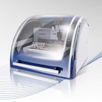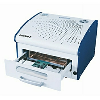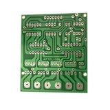

Milling the conductor pattern
1- & 2-sided PCBs and multilayers
Mechanical and laser systems selectively remove the copper layers on single- and double-sided circuit boards, thereby creating insulating channels that precisely delineate the required conductive traces and pads. The circuit board plotters also drill all the necessary holes in the boards.
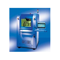
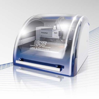
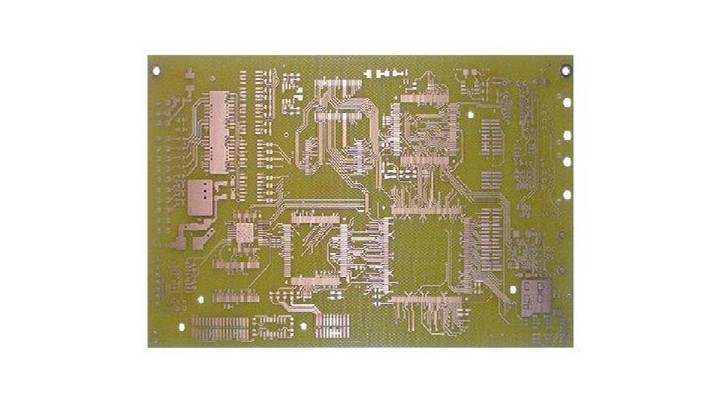
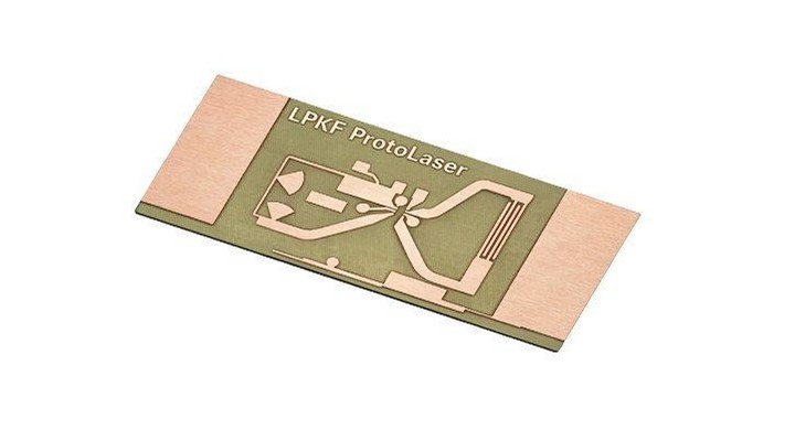
PCB structuring with the laser
1- & 2-sided PCBs and multilayers
Laser structuring implements conductive paths even faster and more accurately than mechanical methods do. It places exact geometries on various substrates such as copper-clad FR4, aluminized PET film, ceramics, duorid or PTFE.